Synopsys
EDA Tools · Workforce Development Partner

GlobalFoundries
GF180nm Fabrication · MoU Partner
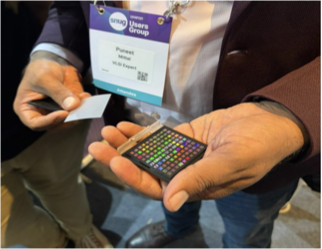
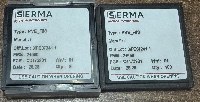
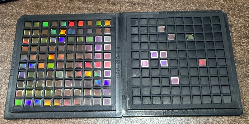
Nine students from Tier 2 and Tier 3 colleges designed a Mini Processor from scratch, fabricated it on real silicon using GlobalFoundries 180nm process, and held the finished chip in their hands. VLSI EXPERT became the first private finishing training institute in India to ever do this.
Until now, real chip fabrication in India happened in two places: inside universities with research grants, or inside semiconductor companies with production budgets. Nobody had done it through a private training institute — until a group of nine students from ordinary engineering colleges decided they would.
There is a moment that every semiconductor engineer dreams about — the moment a physical chip, one that came from your own design, arrives in your hands. It is smaller than a fingernail. It weighs almost nothing. And yet holding it feels like holding something enormous, because you know exactly what went into it: months of late nights, failed simulations, re-runs, debugging sessions that stretched past midnight, and a stubborn refusal to give up.
When that moment arrived for nine students from VLSI EXPERT's ChipTapeout program, it was different from any chip that had been taped out at a training institute before. Because no training institute had done it before. Not in India. Not at this scale. Not with students from Tier 2 and Tier 3 colleges who had never touched a fabrication flow in their lives before joining this program.
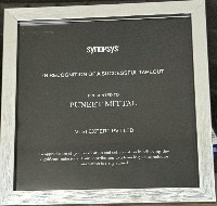
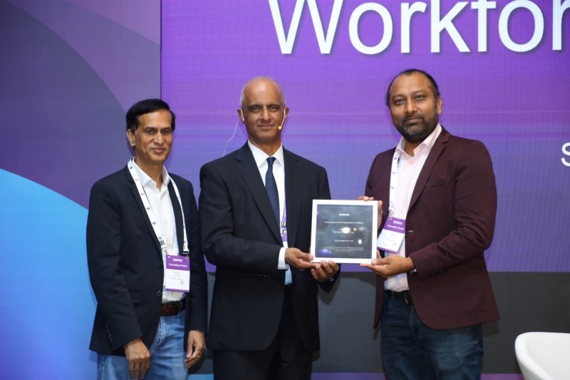
The chip they held was a Mini Processor — designed entirely by them, from specification to GDSII, simulated using Synopsys VCS, physically implemented using IC Compiler II, and fabricated on GlobalFoundries GF180nm process. It was real silicon. It worked. And Synopsys recognised it at SNUG India.
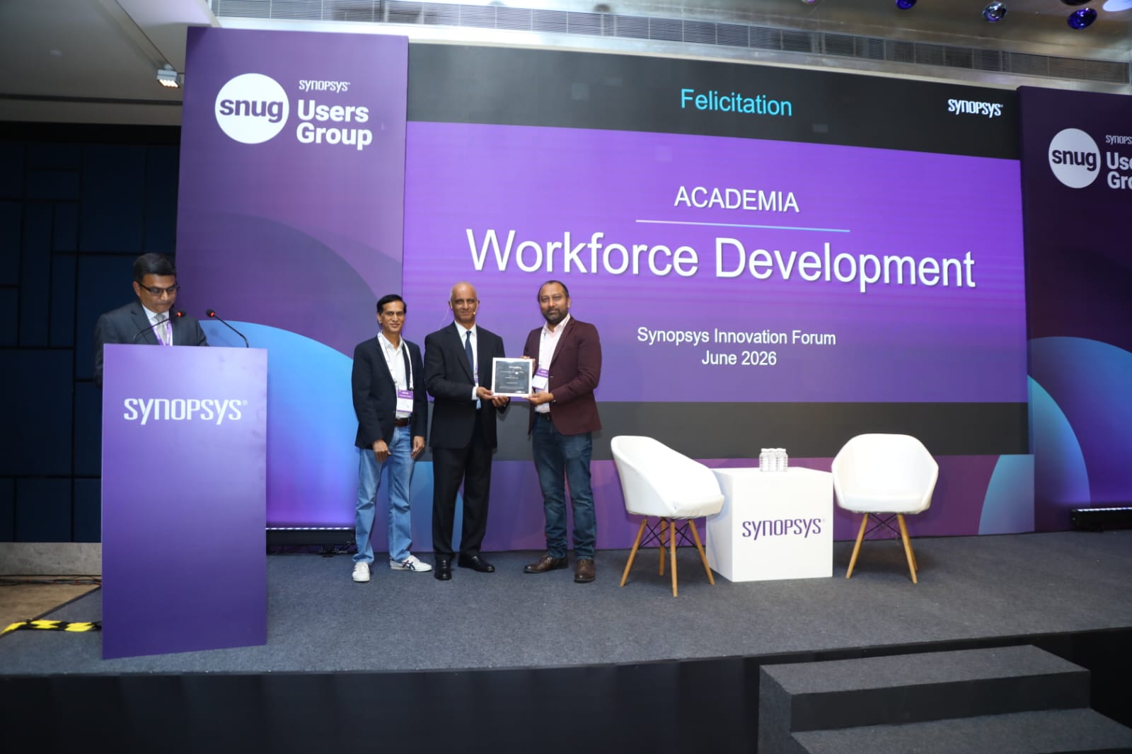
Chip fabrication is expensive, technically demanding and institutionally complex. Universities have done it through sponsored research programs. Companies do it because it is their core business. But a private training institute — one whose students come from all over India, from colleges whose names don't appear on any IIT list — taking nine students through a complete tapeout in 3.5 months? That had never happened.
The reason it had not happened is not hard to understand. The risk is enormous. The tools require deep expertise to use correctly. The process nodes have strict design rules. A single error late in the flow can invalidate weeks of work. And students — especially students without prior chip design experience — are not supposed to be able to do this in 3.5 months.
That last assumption is what VLSI EXPERT set out to disprove.
Either everyone gets a chance to do real work, or we are just teaching theory and calling it training. I wanted these students to hold a chip they had designed. Not a simulation screenshot. Not a layout screenshot. A chip.
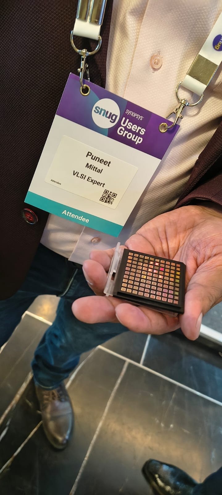
A Mini Processor is not a simple design. It requires a complete RTL implementation, a working testbench, functional simulation, synthesis, physical design including floorplanning, placement and routing, static timing analysis, DRC and LVS clean signoff, and finally GDSII generation for the foundry. Every stage of that flow was done by the students themselves — mentored, guided and reviewed by Puneet Mittal, Dr. Kanika Nagpal and industry engineers, but executed by the students.
The fact that it came back from fabrication working — that it was recognised by Synopsys at SNUG India — tells you everything about the quality of the work.
The nine students were organised into three teams of three. Each team worked on a different module of the processor, then integrated their work into the final design. This is how real chip teams operate inside companies — not one person doing everything, but specialists working in parallel and then coming together.









The schedule was brutal by any reasonable measure. Three and a half months to go from a blank sheet to a GDSII file ready for fabrication. Most university courses take a full academic year to cover the same material, without actually taping out. These students did both.
There were nights when a simulation would not converge. Nights when the timing constraints refused to close. Nights when a DRC run would throw hundreds of violations and the team would have to trace each one back to its source. The students worked through all of it — calling in at midnight, sharing screenshots in group chats at 2 AM, debugging together across cities.
I have seen a lot of student projects in my career. What these nine students did in 3.5 months — under real tool conditions, under real design constraints, with a real chip at the end — is not something I expected to see from students at this stage of their careers. It genuinely surprised me.


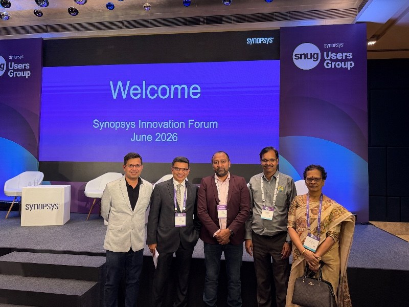
All nine students came through the VLSI EXPERT Foundation of VLSI Design program before being selected for the ChipTapeout intensive. They are not from IITs. They are not from NITs. They are from the kind of colleges that most semiconductor companies would not visit for campus recruitment — colleges where the chip design laboratory, if it exists at all, has tools that are years out of date.
That is the point. The assumption that serious chip design work requires IIT pedigree or premium college infrastructure is exactly the assumption that VLSI EXPERT was built to challenge. The tools are available. The mentorship is available. The methodology can be taught. What was missing was someone willing to take these students seriously and give them the chance.
The ChipTapeout program is not a one-time event. VLSI EXPERT has signed a formal MoU with GlobalFoundries to continue chip fabrication programs for students. The next cohort is being planned — and this time, the bar is set higher because the first group proved it is possible.
For the nine students who taped out this chip: the chip on your desk is proof that where you come from does not determine what you can build. It is proof that with the right environment, the right mentorship and the right determination, students from any college in India can do work at the highest level of the semiconductor industry.
They are not just trained. They are engineers. And they have a chip to prove it.
This is what we built VLSI EXPERT for. Not to teach slides about VLSI. To produce engineers who can sit next to any IIT graduate in a chip design team and outwork them. These nine students just did that — and they did it by taping out real silicon.